Types of LEDs
Packages, power classes, display technologies and specialty emitters, with specs and side-by-side comparisons
LEDs are grouped by package (how the chip is housed and mounted: through-hole, surface-mount, chip-on-board, chip-scale), by power class (indicator, mid-power, high-power), by function (lighting, display, sensing) and by emission (visible, infrared, ultraviolet, multi-color, addressable). The package largely determines how much heat an LED can shed, and therefore how bright and efficient it can be.
The same blue InGaN chip can end up in a 5 mm indicator, a 2835 strip LED, a 100 W COB floodlight or a MicroLED TV. What changes is the package: how the die is mounted, wired, covered with phosphor and, most importantly, cooled. This guide covers every major family with its dimensions, typical power, light output and best uses, and ends with a sortable master comparison table.
Through-hole (DIP) LEDs: 3 mm and 5 mm
Through-hole, or DIP, LEDs are the classic epoxy-bullet LEDs with two wire legs, mainly 3 mm (T-1) and 5 mm (T-1¾). They run at about 20 mA and 0.1 W or less, and because heat can leave only through the thin leads, they suit indicators, hobby electronics and large-pixel signs rather than lighting.
The through-hole or DIP LED is the iconic LED: an epoxy bullet with two wire legs that go through holes in a circuit board. The two standard sizes are 3 mm (T-1) and 5 mm (T-1¾), with 8 mm and 10 mm versions for larger indicators. The epoxy body is both the package and the lens. The shape of its dome sets the viewing angle, from a narrow 15° for bright "water-clear" LEDs to 60°+ for diffused ones.
Anatomy and polarity
The die sits in a reflector cup on one lead and connects to the other through a gold bond wire thinner than a hair. To find polarity, the anode (+) lead is longer, the cathode (−) side has a flat spot on the rim, and the larger internal electrode is usually the cathode.
Inside, the LED die sits in a tiny reflector cup on top of one lead (the anvil, usually the cathode) and is connected to the other lead (the post, the anode) by a gold bond wire thinner than a human hair. To identify polarity: the anode (+) lead is longer, the cathode (−) side has a flat spot on the rim, and the larger internal electrode is usually the cathode.
| Parameter | 3 mm / 5 mm indicator | 5 mm "high-brightness" white |
|---|---|---|
| Typical forward current | 20 mA (max ~30 mA) | 20–30 mA |
| Forward voltage | 1.8–2.2 V (red/yellow) · 2.8–3.4 V (blue/green/white) | 2.9–3.4 V |
| Power | ~0.04–0.1 W | ~0.1 W |
| Output | a few to ~30,000 mcd (narrow beam) | ~5–20 lm |
| Thermal path | Leads only (poor) | Leads only (poor) |
Variants: diffused, straw hat, piranha, flashing
Diffused DIP LEDs spread light evenly while water-clear lenses give a bright narrow beam. Straw-hat LEDs have a wide 100–120° beam, four-lead piranha or superflux LEDs carry 50–80 mA for older tail lights, and flashing or color-cycling LEDs contain a tiny chip that blinks or fades them automatically.
- Diffused vs. water-clear: diffused epoxy scatters light for even, wide-angle indicators. Clear lenses give a bright, narrow beam.
- Straw-hat LEDs have a short, wide dome for a 100–120° beam and are common in signage and cheap lamps.
- Piranha (superflux) LEDs are square, four-lead packages that spread heat through four pins and carry 50–80 mA. They were the standard for automotive tail lights before SMD.
- Flashing and color-cycling LEDs contain a tiny integrated circuit that blinks or fades the LED on its own.
DIP LEDs are still ideal for hobby electronics, panel indicators and outdoor full-color signs with large pixel pitch, where their sealed epoxy body is robust. But because heat can only leave through thin leads, they cannot be driven hard. For illumination they have been replaced almost entirely by SMD packages.
Pros
- Cheap, robust, sealed epoxy body
- Easy to hand-solder and breadboard
- Built-in lens gives a bright, narrow beam
- Huge choice of colors, sizes and angles
Cons
- Heat leaves only through thin leads, so ~0.1 W maximum
- Poor efficacy for room lighting
- Through-hole assembly costs more than SMD in volume
Real examples: Cree C503 series 5 mm LEDs, Kingbright WP7113 series indicators, Vishay TLHR5400 (5 mm red), and the 5 mm LEDs in almost every hobby electronics kit.
SMD (surface-mount) LEDs
Surface-mount (SMD) LEDs sit flat on the circuit board and are soldered to copper pads by machine. Most lighting types are PLCC packages, a lead frame in a reflective white housing filled with phosphor silicone, and their thermal pads shed heat far better than DIP LEDs, so they dominate bulbs, tubes, panels and strips.
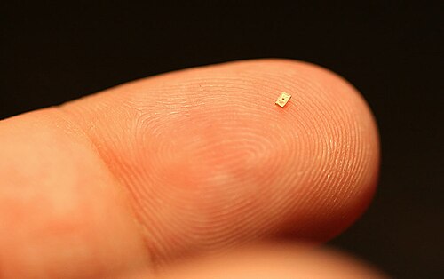

Surface-mount device (SMD) LEDs sit flat on the circuit board and are soldered to pads by machine. Most lighting-grade SMD LEDs are PLCC (plastic leaded chip carrier) packages. A white reflective plastic or epoxy housing surrounds a metal lead frame, and the cavity is filled with silicone and phosphor. Because the lead frame, and in good packages a dedicated thermal pad, sits directly on copper, SMD LEDs shed heat far better than DIP LEDs. This is why they took over bulbs, tubes, panels, strips and backlights.
How SMD names work
An SMD LED's four-digit name is its footprint in tenths of a millimeter: a 2835 measures 2.8 × 3.5 mm and a 5050 measures 5.0 × 5.0 mm. The name says nothing about power or quality. Tiny indicator LEDs use imperial resistor-style codes such as 0603, which equals metric 1608.
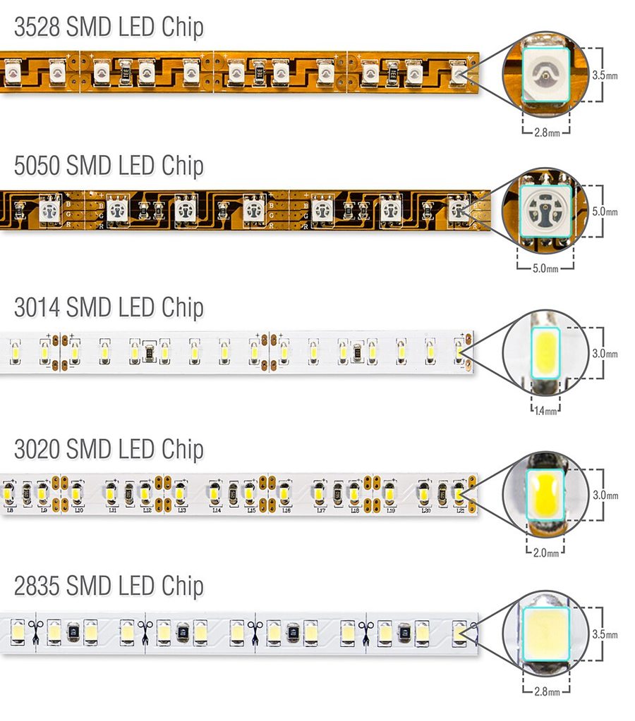

The four-digit name is simply the footprint in tenths of a millimetre: a 2835 is 2.8 × 3.5 mm and a 5050 is 5.0 × 5.0 mm. The name says nothing about power or quality. Two "2835" LEDs can differ fivefold in output and efficiency depending on chip, current and brand. Tiny chip LEDs for indicators use the resistor-style imperial codes 0402, 0603, 0805, 1206. Watch the confusion: imperial 0603 equals metric 1608 (1.6 × 0.8 mm).
| Package | Size (mm) | Typical power | Typical flux (white) | Thermal pad | Typical use |
|---|---|---|---|---|---|
| 3528 | 3.5 × 2.8 × 1.9 | 0.06–0.08 W (20 mA) | 5–8 lm | No | Early low-power strips, backlights, indicators |
| 2835 | 2.8 × 3.5 × 0.8 | 0.2 W (60 mA); 0.5 W and 1 W versions | 20–30 lm at 0.2 W; up to ~130 lm at 1 W | Yes (large) | Bulbs, tubes, panels, high-efficiency strips |
| 3030 | 3.0 × 3.0 × 0.55 | 0.5–2 W | 60–250 lm | Yes | High-bays, streetlights, horticulture boards |
| 5050 | 5.0 × 5.0 × 1.6 | 0.2–0.24 W (3 × 20 mA) | 18–24 lm | No (6 leads) | RGB and addressable strips, signage |
| 5630 | 5.6 × 3.0 × 0.9 | 0.5 W (150 mA) | 45–60 lm | Yes (centre) | Panels, troffers, T8 tubes |
| 5730 | 5.7 × 3.0 × 0.8 | 0.5–1 W | 50–60 lm at 0.5 W | Yes | Corn bulbs, panels, tubes |
Interactive diagram: SMD LED footprints drawn to scale, with thermal pads
2835 vs. 5050: which is better?
For white light, 2835 is better: its single chip on a large thermal pad reaches 120–200+ lumens per watt, so 2835 strips are brighter and cooler at the same wattage. The 5050 holds three dies, making it the natural choice for RGB and addressable pixels such as the WS2812B.
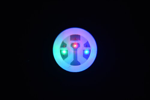

For white light, the 2835 wins. Its single chip on a large thermal pad reaches 120–200+ lm/W, so a 2835 strip at the same wattage is brighter and runs cooler. The 5050 holds three dies, which makes it the natural package for RGB (one red, green and blue die each) and for addressable pixels such as the WS2812B with a controller chip inside. For tunable white, RGBW and RGBCCT strips, both are common, along with larger 5050 variants carrying four or five dies.
Housing materials: PPA, PCT and EMC
SMD LED housings are made of PPA, PCT or EMC plastic. PPA, used in early and budget packages, yellows under heat and blue light; PCT resists this better; and EMC epoxy molding compound, used in modern 3030 and high-current 2835 LEDs, tolerates far higher temperatures and currents, a hidden mark of quality.
Early PLCC housings used PPA (polyphthalamide), which yellows under heat and blue light and limits drive current. PCT resists this better. EMC (epoxy molding compound), used in modern 3030 and high-current 2835 packages, tolerates much higher temperatures and currents. It is a hidden but significant difference between budget and premium LEDs.
Pros
- Machine-placed and very cheap at scale
- Thermal pads let mid-power packages reach 120–220 lm/W
- Low profile for strips, panels, tubes and bulbs
- Every CCT and CRI grade available
Cons
- Package names say nothing about power or quality
- PPA housings yellow when overdriven
- Many small points of light cause multiple shadows and glare without a diffuser
Real examples: Samsung LM281B+ (2835), Samsung LM301B and LM301H (3030, common on horticulture boards), Nichia NF2W757 (3030), and the Lumileds LUXEON 2835 and 3030 2D lines. Full comparison: SMD 2835 vs 5050 vs 3030.
Inside the package: DIP vs. SMD vs. COB
DIP, SMD and COB packages differ mainly in how heat leaves the die. A DIP LED sheds heat through a thin lead, an SMD LED through a metal pad soldered to the board, and a COB through a thick metal or ceramic substrate bolted directly to a heat sink.
The three main package styles differ mostly in how they get heat out of the die. In a DIP LED, heat has to travel down a thin lead. An SMD LED sits on a metal pad soldered straight to the board. A COB places many bare dies directly on a thick metal or ceramic substrate that bolts to a heat sink. Chip-scale packages, which remove the package altogether, are compared with both in COB vs SMD vs CSP.
Interactive diagram: DIP, SMD and COB cross-sections compared
COB and MCOB LEDs
Chip-on-board LEDs bond dozens to hundreds of bare dies directly onto an aluminum or ceramic substrate under one continuous phosphor layer, creating a single uniform light-emitting surface 6–30 mm across. Rated from 3 to over 200 W, they power downlights, spotlights, high-bays and stage lights, and need generous heat sinks.
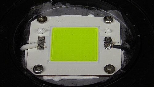

Chip-on-board (COB) LEDs skip the individual package. Dozens to hundreds of bare dies are bonded directly to an aluminium or ceramic substrate, wired in series-parallel strings, surrounded by a dam ring and covered with one continuous layer of phosphor silicone. The result is a single, uniform light-emitting surface (LES), often 6–30 mm across, that behaves like one bright source.
- Power: 3–200 W+ per module, at 9–48 V or more depending on string length.
- Uses: downlights, track spotlights, retail and museum lighting, high-bays, stage fixtures, and the "corn" and GU10 retrofit lamps.
Pros
- Very high lumen density for tight beams from small reflectors
- One clean shadow instead of multi-shadows
- Excellent color uniformity and high-CRI options (Ra 95–98)
- Simple assembly: one part, two wires
Cons
- All the heat is concentrated in a small area, so COBs need generous heat sinks
- Efficacy slightly below the best mid-power SMD arrays
- A failed string dims or darkens the whole module
Real examples: Cree XLamp CXA and CXB series, Bridgelux Vero and V Series, Citizen CLU series and Lumileds LUXEON CoB, found in museum track spots, high-CRI downlights and stage fixtures.
MCOB (multi-chips-on-board) usually refers to several COB clusters on one board, common in decorative and corn bulbs. COB LED strips ("dotless" strips) apply the same idea to flexible tape: 300–500+ tiny dies per metre under a continuous phosphor line give a seamless line of light with no visible dots, even without a diffuser.
CSP (chip-scale package) and flip-chip LEDs
A chip-scale package LED is no more than 20% larger than its die: a flip-chip die solders directly to the board, with phosphor applied as a thin film and no lead frame, bond wires or housing. CSPs are tiny, run cool and suit backlights, headlamps, camera flashes and dense arrays.
A chip-scale package (CSP) LED is barely larger than the die itself. By common definition the package is no more than 20% bigger than the chip. It uses a flip-chip die: instead of being wired from the top, the chip is flipped so both electrodes on its underside solder directly to the board. Phosphor is applied as a thin film or molded shell around the die. There is no lead frame, no bond wires and no plastic housing.
Benefits are extreme compactness (1–1.5 mm square), very low thermal resistance straight into the PCB, no wire-bond failures and high current density. That makes CSPs ideal for TV and monitor backlights, automotive headlamps and compact retrofit bulbs, camera flashes and dense arrays. The trade-offs are side emission (some blue escapes at the edges unless managed), demanding solder-assembly accuracy, and sensitivity to board quality because there is no package to buffer stress.
Pros
- Smallest possible footprint, 1–1.5 mm square
- Lowest thermal resistance into the board
- No bond wires to break
- High luminance for compact optics
Cons
- Blue light can leak from the sides
- Demanding solder assembly and board flatness
- No package to buffer mechanical stress; hard to rework
Real examples: Lumileds LUXEON FlipChip, Seoul Semiconductor WICOP, and the CSP arrays inside many direct-lit TV backlights, phone camera flashes and LED headlamps.
Filament LEDs (COG)
LED filaments are narrow glass or sapphire strips carrying 20–30 tiny dies in series, coated with phosphor so they glow in every direction, recreating the look of a clear Edison bulb. A four-filament lamp gives about 400–470 lumens, at 100–160 lumens per watt, but enclosed fixtures shorten their life.
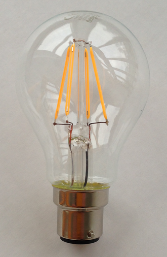

The LED filament recreates the look of a classic clear Edison bulb. Each filament is a narrow strip of glass, sapphire or flexible substrate about 1 mm wide and 25–40 mm long, carrying 20–30 tiny dies in series (hence COG, chip-on-glass) and coated all round with phosphor silicone so it glows in every direction. A filament typically runs at about 1 W and 60–80 V. A 4-filament lamp gives about 400–470 lm, and an 8-filament lamp about 800–1,000 lm.
The bulb is often filled with a helium-rich gas to carry heat from the filaments to the glass, because there is no heat sink. Filament lamps reach 100–160 lm/W, combine 360° light with a vintage look, and are popular in pendants, chandeliers and exposed-bulb fixtures. Flexible "spiral" filaments allow vintage shapes. Avoid enclosed fixtures, which shorten their life, and buy dimmable versions specifically if needed.
Pros
- Classic clear-bulb look with 360° light
- 100–160 lm/W, and above 200 lm/W in the best models
- Warm 2200–2700 K versions suit decorative fixtures
Cons
- No heat sink, so enclosed fixtures shorten life
- A small driver in the base limits flicker and dimming quality
- Bare filaments cause glare at high output
Real examples: Philips (Signify) LED Classic filament bulbs, the Philips Ultra Efficient range at around 210 lm/W, and IKEA LUNNOM decorative filament bulbs.
High-power LEDs (1 W to 100 W+)
High-power LEDs drive a single large die, usually 1 mm square or more, at 350 mA to 3 A in ceramic or metal-slug packages with very low thermal resistance. Starting with the 1999 Luxeon, they became standard in flashlights, headlamps and floodlights, and always need a constant-current driver and heat sink.
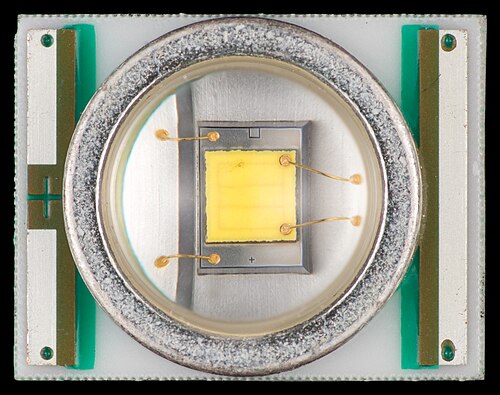

High-power LEDs drive a single large die (typically 1 × 1 mm or bigger) at 350 mA to 3 A or more. They are built on ceramic (aluminium nitride or alumina) or metal-slug packages with a silicone dome lens, and very low thermal resistance (under 3–6 K/W junction-to-pad). The lineage starts with the 1999 Lumileds Luxeon. Cree's XLamp XR-E (2006), XM-L (2010) and multi-die XHP series made them standard in flashlights, bike lights, automotive headlamps and architectural floodlights.
- 1–3 W emitters such as the 3535 or 5050 ceramic: 100–350 lm each, usually supplied on a 16 or 20 mm aluminium "star" board.
- Multi-die emitters (6 V and 12 V versions): up to ~4,000 lm from a 7 × 7 mm package.
- 10–100 W arrays and COBs for floodlights, high-bays, grow lights and stage fixtures, and 200 W+ modules for stadium floodlights.
High-power LEDs always need a constant-current driver and a heat sink. Efficacy peaks at moderate current, so efficient designs often run more emitters gently instead of a few hard (see efficiency droop).
Pros
- High output from one point source, ideal for tight beams
- Ceramic packages with very low thermal resistance
- Long LM-80 test histories and stable color
Cons
- Needs a constant-current driver and a real heat sink
- Efficacy falls at high current (droop)
- Intense point source causes glare without optics
Real examples: Cree XLamp XP-G3, XM-L2 and XHP70.2, Lumileds LUXEON Rebel and LUXEON V, ams OSRAM OSLON Square, and the high-CRI Nichia 219 series used in enthusiast flashlights.
OLED: organic light-emitting diodes
OLEDs replace crystalline semiconductors with organic molecule layers only 100–500 nm thick, deposited on glass or flexible plastic. Every sub-pixel makes its own light and can switch fully off, giving perfect blacks, which is why OLED dominates flagship phones and premium TVs despite fast-aging blue emitters and burn-in risk.
An OLED replaces crystalline semiconductors with thin layers of organic (carbon-based) molecules, about 100–500 nm thick in total, sandwiched between a transparent anode (ITO) and a metal cathode. Electrons and holes recombine in the emissive layer to form excitons that emit light. Modern phosphorescent emitters harvest nearly 100% of excitons for red and green, while blue still relies on less efficient fluorescent or TADF emitters. Because OLEDs can be deposited on glass or flexible plastic over large areas, they are ideal for displays in which every sub-pixel makes its own light and can switch fully off for perfect black.
AMOLED and PMOLED
AMOLED screens give every sub-pixel its own thin-film transistors, keeping it lit for the whole frame; they are used in nearly all flagship phones and smartwatches, and LTPO backplanes allow refresh rates from 1 to 120 Hz. Passive-matrix PMOLED scans rows in turn and suits only small, simple displays.
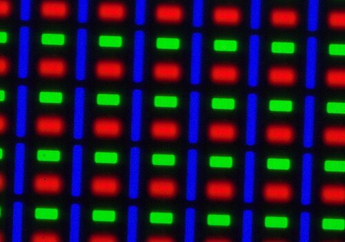

AMOLED (active-matrix OLED) gives each sub-pixel its own thin-film transistors on an LTPS or LTPO backplane, holding it lit for the whole frame. This is the technology in nearly all flagship smartphones and smartwatches. LTPO backplanes allow variable refresh from 1 to 120 Hz to save power. PMOLED (passive matrix) scans rows one at a time and is limited to small, simple displays such as fitness bands and small monochrome screens.
WOLED and QD-OLED (TVs)
Large OLED TVs use two designs. LG's WOLED, sold since 2013, makes white light and filters it into red, green and blue sub-pixels plus an unfiltered white one. Samsung's QD-OLED, since 2022, converts blue OLED light into red and green with quantum dots for purer, brighter colors.
Large OLED TVs use two architectures. WOLED (LG Display, since 2013) stacks blue and yellow-green emitters to make white light, then uses red, green and blue color filters plus an unfiltered white sub-pixel (WRGB) for brightness. QD-OLED (Samsung Display, since 2022) uses a blue OLED layer and converts it to red and green with printed quantum dots, giving purer colors and better brightness on color highlights. Tandem OLED stacks two emissive layers, roughly doubling brightness and lifetime, and is now used in tablets, laptops and cars.
Burn-in
Burn-in is permanent ghosting on an OLED screen. Organic emitters, especially blue, lose efficiency with use, so static logos, tickers or taskbars shown for many hours age those sub-pixels faster than their neighbors. Pixel shifting, logo dimming and compensation cycles make it rare in mixed everyday TV viewing.
Organic emitters slowly lose efficiency with use, and blue fades fastest. If static content such as a news ticker, channel logo, game HUD or taskbar is shown for many hours, those sub-pixels age faster than their neighbors and leave a permanent ghost image: burn-in. Manufacturers fight it with pixel shifting, logo detection and dimming, compensation cycles that measure and correct aging, heat sinks, and tandem stacks. For mixed everyday viewing, modern OLED TVs rarely show burn-in. For static signage or desktop use, LCD and MicroLED remain safer.
OLED lighting panels also exist as thin, glare-free area lights at 50–90 lm/W, used in design luminaires and in some automotive tail lights, but they remain a niche compared with inorganic LEDs.
Pros
- Perfect black and per-pixel contrast
- Thin, light, flexible and foldable panels
- Wide viewing angles and fast pixel response
Cons
- Burn-in risk with static content
- Lower full-screen brightness than Mini-LED LCDs
- Blue emitters age fastest; costly at large sizes
Real examples: AMOLED screens in Samsung Galaxy phones and every iPhone since the iPhone X (2017), LG OLED C- and G-series TVs (WOLED), Samsung S95B and Sony A95K QD-OLED TVs (2022), and the tandem-OLED iPad Pro (2024). How the four display technologies compare: OLED vs QLED vs Mini-LED vs MicroLED.
QLED and quantum-dot displays
QLED is a marketing name, mainly Samsung's, for LCD TVs with a quantum-dot layer; they are not self-emissive. A blue LED backlight excites 2–10 nm nanocrystals that emit pure red and green, giving wide color gamut and high brightness. True electroluminescent quantum-dot LEDs are still in development.
"QLED" is a marketing term, mainly Samsung's, for LCD televisions with a quantum-dot layer. They are not self-emissive. A blue LED backlight shines through a quantum-dot enhancement film (QDEF) containing nanocrystals, about 2–10 nm across and made of indium phosphide or cadmium selenide, whose size sets their emission. Smaller dots emit green and larger dots emit red. The result is very pure red and green light, which lets the LCD's color filters reproduce a wide color gamut (90%+ of DCI-P3) at high brightness.
True electroluminescent quantum-dot LEDs (QD-LEDs or "QDEL"), in which the dots themselves are driven electrically like an OLED, are under active development and promise emissive displays without organic-emitter aging, but they are not yet a mainstream product. In QD-OLED the dots act only as color converters for a blue OLED.
Pros
- Very bright, with no burn-in
- Wide color gamut (90%+ of DCI-P3)
- Cheaper than OLED at large sizes
Cons
- Still an LCD: greyish blacks without local dimming
- Narrower viewing angles on VA panels
- The name is easily confused with OLED
Real examples: Samsung's QLED TV ranges (since 2017), plus quantum-dot LCD TVs from TCL, Hisense and others, many of which now pair quantum dots with a Mini-LED backlight.
Mini-LED
Mini-LED is an LCD backlight made of thousands of LEDs 50–200 µm across, grouped into hundreds or thousands of local-dimming zones that follow the image. It delivers HDR highlights of 1,000–2,000+ nits and deep blacks without burn-in, though bright objects on dark backgrounds can show faint blooming halos.
Mini-LED is an LCD backlight built from thousands of very small LEDs, typically 50–200 µm dies, grouped into hundreds to thousands of local-dimming zones. Each zone brightens or dims to follow the image, so dark areas get darker and highlights brighter. Full-array local dimming (FALD) with Mini-LEDs gives HDR peaks of 1,000–2,000+ nits and contrast approaching OLED, at lower cost and with no burn-in risk. The 2021 12.9-inch iPad Pro, for example, used over 10,000 Mini-LEDs in 2,596 zones.
The main artifact is blooming, a faint halo around bright objects on dark backgrounds, because each zone still covers many pixels. More zones and better algorithms reduce it. "Mini-LED" also describes fine-pitch direct-view LED video walls (pixel pitch under ~1 mm), which bridge to MicroLED.
Pros
- HDR peaks of 1,000–2,000+ nits
- Deep blacks with many dimming zones
- No burn-in; cheaper than OLED at large sizes
Cons
- Blooming halos around bright objects
- Zone algorithms can lag fast content
- Thicker and heavier than OLED panels
Real examples: the 12.9-inch iPad Pro and the 14- and 16-inch MacBook Pro (both 2021), Samsung Neo QLED TVs, and Mini-LED TVs from TCL (first in 2019) and Hisense.
MicroLED
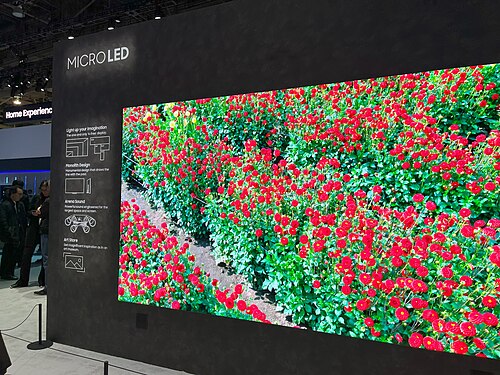
MicroLED displays build every sub-pixel from its own microscopic inorganic LED, usually under 50 µm. They combine OLED's perfect blacks with inorganic LEDs' brightness and decades-long life, but a 4K screen needs about 24.9 million working dies placed by mass transfer, so today's MicroLED screens remain extremely expensive.
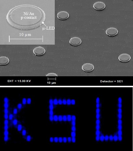

MicroLED displays make every sub-pixel from its own microscopic inorganic LED, typically under 50 µm and down to a few microns for AR microdisplays. It combines OLED's per-pixel control and perfect blacks with the brightness, efficiency and lifetime of inorganic LEDs. There is no burn-in, brightness can exceed several thousand nits, and the display lasts for decades.
The challenge is manufacturing. A 4K screen needs about 24.9 million sub-pixels (3840 × 2160 × 3), each one a separately grown, tested and placed LED. Mass transfer has to move millions of dies per hour with near-perfect yield, and every dead pixel must be repaired. Red micro-LEDs are particularly inefficient at small sizes, because surface recombination at the die edges grows as the die shrinks. Modular MicroLED walls (Samsung's "The Wall", 2018) and very expensive large TVs exist. Monolithic MicroLED microdisplays for AR glasses are shipping in small volumes. Affordable MicroLED phones and TVs remain a goal for the late 2020s and beyond.

Pros
- Perfect blacks with very high brightness
- No burn-in; decades of life
- Modular, seamless walls of any size
Cons
- Extremely expensive
- Mass transfer and repair are hard at scale
- Red micro-LEDs lose efficiency as they shrink
Real examples: Samsung The Wall (2018) and its 110-inch MicroLED TV (2021), LG MAGNIT, Sony Crystal LED video walls, and monolithic MicroLED microdisplays in AR glasses.
Infrared LEDs: 850 nm vs. 940 nm
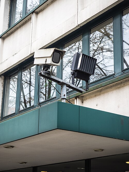
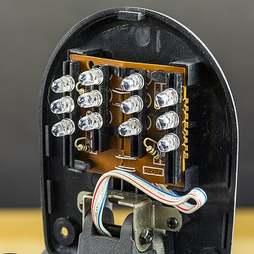
Infrared LEDs made from GaAs and AlGaAs emit mainly between 700 and 1,000 nm. 850 nm parts show a faint red glow but give silicon cameras longer night-vision range, while 940 nm parts are invisible and suit remote controls, covert cameras and sensors. They are rated in milliwatts, not lumens.
Infrared (IR) LEDs, made of GaAs and AlGaAs, emit beyond the visible red, mostly between 700 and 1,000 nm, with special InGaAsP parts out to 1,600 nm for fiber. They are the oldest commercial LEDs (1962) and are still made by the billions. The two workhorse wavelengths:
| 850 nm | 940 nm | |
|---|---|---|
| Visibility | Faint dull-red glow visible to the eye | Invisible ("no-glow", covert) |
| Silicon camera sensitivity | Higher; longer night-vision range | Roughly 40–60% lower; shorter range for the same power |
| Sunlight interference | More | Less (atmospheric water absorbs near 940 nm) |
| Typical uses | CCTV and dash-cam illuminators, PBM therapy, machine vision, short fiber links | TV and AC remotes, proximity and gesture sensors, covert cameras, pulse oximetry, face-recognition flood illumination |
IR LEDs are rated in radiant power (mW) or radiant intensity (mW/sr), not lumens. Remote controls modulate a 940 nm LED at a 36–40 kHz carrier so the receiver can reject ambient light. Optocouplers pair an IR LED with a phototransistor to pass signals across thousands of volts of electrical isolation.


Pros
- Invisible light for night vision and sensing
- High wall-plug efficiency, often 30–50%
- Very cheap, long-lived and fast to modulate
Cons
- High-power IR can harm eyes without triggering a blink (IEC 62471)
- 850 nm parts show a faint red glow
- Sunlight interferes outdoors
Real examples: Vishay TSAL6200 (940 nm, 5 mm), ams OSRAM SFH 4550 (850 nm, 5 mm) and the OSLON Black high-power IR emitters used in CCTV and driver-monitoring cameras.
Ultraviolet LEDs: UV-A, UV-B and UV-C
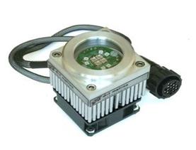
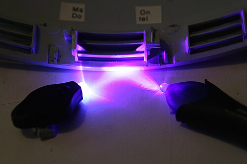
UV LEDs are made from InGaN for near-UV and AlGaN for shorter wavelengths. UV-A at 365–405 nm cures inks, resins and nail gel; UV-B at 280–315 nm treats skin conditions; and UV-C at 255–280 nm disinfects water, air and surfaces, although UV-B and UV-C efficiency is only a few percent.
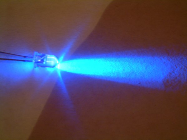

Ultraviolet LEDs are made from InGaN (near-UV) and from AlGaN with increasing aluminium content for shorter wavelengths. They are replacing mercury lamps, which are being phased out under the Minamata Convention, in many uses.
| Band | Range | Common LED wavelengths | Uses | Efficiency |
|---|---|---|---|---|
| UV-A | 315–400 nm | 365, 385, 395, 405 nm | Curing of inks, adhesives, coatings and nail gel; 3D-printer resin; fluorescence, forensics, counterfeit detection; insect traps | WPE 20–60% |
| UV-B | 280–315 nm | 295–311 nm | Phototherapy (psoriasis, vitiligo), plant UV-B research, vitamin D studies, sensing | WPE ~1–5% |
| UV-C | 100–280 nm | 255–280 nm (265 and 275 most common) | Germicidal disinfection of water, air and surfaces; DNA/RNA damage stops microbe replication; spectroscopy | WPE ~2–10% |
UV-C and UV-B are hazardous to eyes and skin: they cause photokeratitis ("welder's flash") and erythema within seconds to minutes at close range. UV-C devices must be enclosed or interlocked. Many consumer "UV-C" gadgets emit far too little UV-C to disinfect, or are really UV-A, so look for stated irradiance (mW/cm²) and tested log-reduction data.


Pros
- Mercury-free, compact and instant-on
- Wavelengths chosen for the job: 365–405 nm curing, 265–280 nm disinfection
- Long life, dimmable and unaffected by frequent switching
Cons
- UV-B and UV-C efficiency only a few percent
- Hazardous to eyes and skin
- Many consumer UV-C products are underpowered
Real examples: Nichia NCSU series UV-A LEDs (365 nm), Crystal IS Klaran UV-C LEDs (grown on aluminium nitride), Seoul Viosys violeds, and the 405 nm curing arrays in resin 3D printers.
Addressable LEDs: WS2812B, SK6812 and APA102
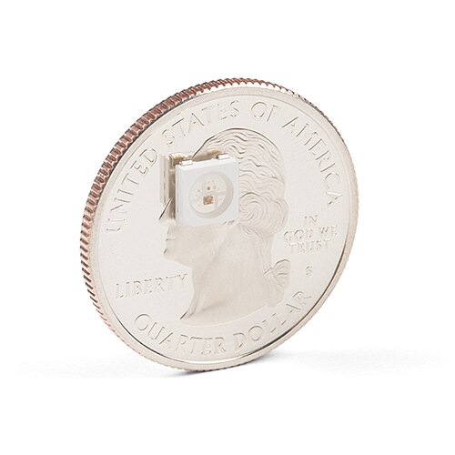
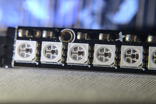
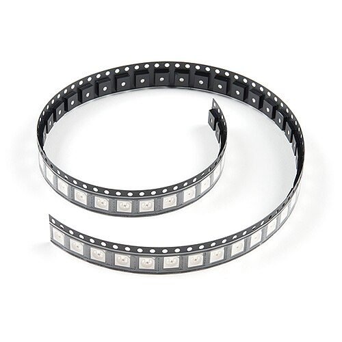
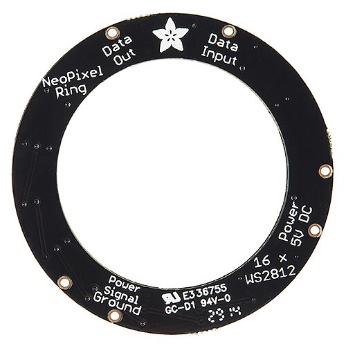
Addressable LEDs such as the WS2812B, SK6812 and APA102 contain a tiny driver chip beside their red, green and blue dies. Each LED reads its own color from a data line and passes the rest along, so every pixel on a strip can show a different color under microcontroller or WLED control.
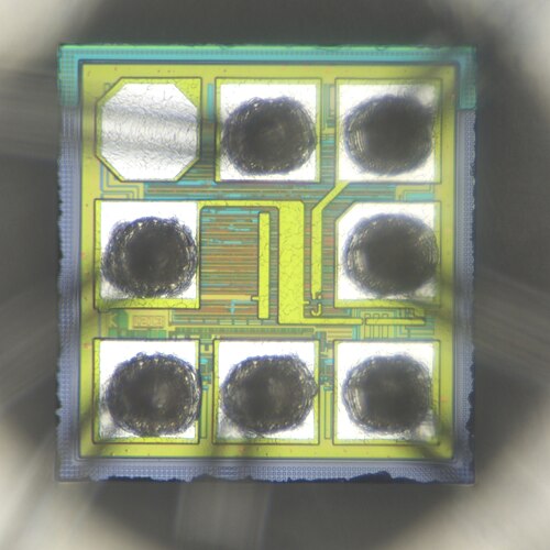

Addressable (or "smart", "pixel", "digital") LEDs contain a tiny driver IC inside the package next to the red, green and blue dies. Each LED receives a color value on a data line, keeps its own share, and passes the rest down the chain, so every pixel on a strip can show a different color. They power gaming setups, DJ booths, art installations, architectural façades and holiday displays, controlled by microcontrollers (Arduino, ESP32) or pixel controllers running WLED, xLights or DMX/Art-Net.
| Chip | Interface | Colors | Voltage | PWM rate | Notes |
|---|---|---|---|---|---|
| WS2812B | 1-wire, 800 kbit/s, timing-critical | RGB, 24-bit (GRB order) | 5 V | ~0.4–2 kHz | The "NeoPixel" standard; ~60 mA at full white per pixel |
| WS2813 / WS2815 | 1-wire + backup data line | RGB | 5 V / 12 V | ~2 kHz | A dead pixel doesn't break the chain; 12 V reduces voltage drop |
| SK6812 (RGBW) | 1-wire, WS2812-compatible timing | RGB + white (warm, neutral or cool), 32-bit | 5 V | ~1 kHz | A real white die gives far better whites and pastels |
| APA102 / SK9822 | 2-wire SPI (data + clock) | RGB + 5-bit global brightness | 5 V | ~19–20 kHz (APA102) | Fast, timing-tolerant, flicker-free on camera, ideal for POV |
Power planning matters. 60 WS2812B LEDs per metre at full white draw about 3.6 A per metre at 5 V. Inject power every 1–2 m (5 V) or use 12 V chips for long runs. Add a 300–500 Ω resistor in the data line and a large capacitor across the supply at the strip input, and use a level shifter when driving 5 V pixels from 3.3 V controllers.




Pros
- Every pixel controllable from one data line
- Driver built into each LED
- Huge ecosystem: Arduino, ESP32, WLED, xLights
- Easy to cut, chain and bend
Cons
- 5 V strips need power injection on long runs
- WS2812B timing is strict and its PWM can flicker on camera
- White from RGB alone looks bluish and renders color poorly
- One dead pixel can stop the chain (except WS2813/WS2815)
Real examples: Worldsemi WS2812B and WS2815, SK6812 RGBW, and APA102 and SK9822 pixels, sold as Adafruit NeoPixel and DotStar products and in countless gaming, holiday and architectural strips.
Bi-color, tri-color, RGB, RGBW and RGBCCT
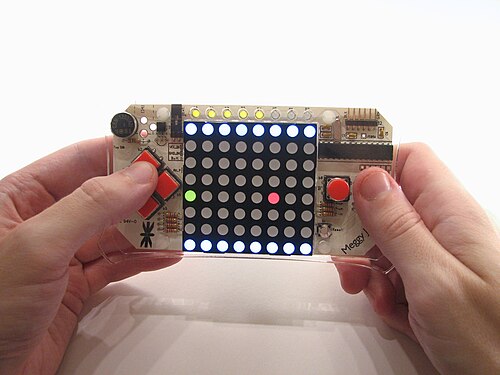
Multi-color LEDs put several dies in one package. Bi-color and tri-color types show status states, RGB mixes millions of colors, RGBW adds a phosphor-white die for real whites, CCT or tunable white blends warm and cool white, and five-channel RGBCCT combines full color with tunable white.

- Bi-color: two dies in one package. In 2-lead versions they are wired back-to-back, so polarity selects red or green. 3-lead versions share a common lead and can show both (yellow/amber).
- Tri-color: three indication states, typically red, green and their mix, or three separate dies, used for status lights (charging, ready, fault).
- RGB: red, green and blue dies with common-anode or common-cathode wiring, mixing millions of colors with PWM. White from RGB alone looks bluish-pink and renders colors poorly.
- RGBW: RGB plus a phosphor-white die, giving real whites (CRI 80–90) and soft pastels. The white can be warm, neutral or cool.
- CCT (tunable white): warm-white and cool-white dies on two channels, blended from about 2,700 to 6,500 K.
- RGBCCT (RGBWW, 5-in-1): RGB plus warm and cool white on five channels: full color plus tunable white, the most flexible choice for smart homes and hospitality.
Master comparison table
Across LED types, mid-power SMD 2835 and 3030 packages lead white-light efficacy at 120–220 lumens per watt, COBs offer the highest CRI options, and high-power and CSP emitters handle heat best. Legacy incandescent bulbs manage only 10–17 lumens per watt; the sortable table compares every type side by side.
Sort by any column, search, or filter by category. Values are typical ranges for current-generation products. Display and specialty emitters show "—" where lumens per watt is not a meaningful metric.
| Type | Efficacy (lm/W) | Lifespan (h) | CRI | Heat handling | Cost | Typical applications |
|---|---|---|---|---|---|---|
| DIP 3 / 5 mm | 20–90 | 20,000–50,000 | 65–80 | Poor (leads only) | $ | Indicators, hobby electronics, large-pitch signs |
| Piranha / superflux | 40–80 | 30,000–50,000 | 65–80 | Fair (4 leads) | $ | Older tail lights, signage, accent |
| SMD 3528 | 60–100 | 25,000–50,000 | 70–90 | Fair | $ | Low-output strips, backlights |
| SMD 2835 | 120–220 | 35,000–60,000 | 80–97 | Good (thermal pad) | $ | Bulbs, tubes, panels, efficient white strips |
| SMD 3030 (EMC) | 150–220 | 50,000–100,000 | 70–90 | Very good | $$ | High-bays, streetlights, horticulture |
| SMD 5050 (white) | 70–110 | 30,000–50,000 | 70–90 | Fair | $ | Signage, legacy strips, tunable/RGBW strips |
| SMD 5630 / 5730 | 100–150 | 30,000–50,000 | 70–90 | Good | $ | Panels, troffers, T8 tubes, corn bulbs |
| High-power emitter (1–10 W) | 100–200 | 50,000–100,000 | 70–95 | Excellent with heat sink | $$ | Flashlights, headlamps, floodlights, bike lights |
| COB (10–200 W) | 100–180 | 30,000–60,000 | 80–98 | Needs a large heat sink | $$ | Downlights, spotlights, retail, high-bay, stage |
| CSP (flip-chip) | 130–200 | 50,000+ | 70–90 | Excellent (direct to PCB) | $$ | Backlights, automotive headlamps, flash, dense arrays |
| Filament (COG) | 100–160 | 15,000–25,000 | 80–90 | Fair (gas-cooled bulb) | $ | Decorative clear bulbs, pendants, chandeliers |
| OLED | 40–90 (panels) | 20,000–100,000 | 85–95 (lighting) | Low heat, area source | $$$ | Phones, watches, TVs, design luminaires |
| QLED (QD-enhanced LCD) | — | 50,000–100,000 | — | Good | $$ | TVs, monitors |
| Mini-LED backlight | — | 50,000–100,000 | — | Good | $$$ | HDR TVs, tablets, laptops, monitors |
| MicroLED | — | 100,000 (projected) | — | Good | $$$$ | Premium modular walls, AR microdisplays, watches |
| IR 850 / 940 nm | — (WPE 30–50%) | 50,000+ | n/a | Good | $ | CCTV, remotes, sensors, optocouplers, PBM |
| UV-A 365–405 nm | — (WPE 20–60%) | 10,000–30,000 | n/a | Fair | $$ | Curing, 3D printing, inspection, forensics |
| UV-C 255–280 nm | — (WPE 2–10%) | 5,000–20,000 | n/a | Poor (high heat per mW) | $$$ | Water, air and surface disinfection |
| Addressable 5050 (WS2812B) | 40–80 (white) | 25,000–50,000 | 50–70 (RGB white) | Fair | $$ | Pixel strips, DJ and stage, gaming, art |
| Incandescent | 10–17 | 750–2,000 | 100 | Very hot (~90% IR) | $ | Phased out for general lighting |
| Halogen | 15–24 | 2,000–4,000 | 100 | Very hot | $ | Old spotlights and headlamps |
| CFL | 50–70 | 8,000–10,000 | 80–85 | Warm; contains mercury | $ | Phased out in the EU (2023) |
| Linear fluorescent T8 | 80–100 | 20,000–36,000 | 80–86 | Ballast losses; mercury | $ | Offices and schools, being retrofitted |
| Metal halide | 65–115 | 10,000–20,000 | 65–95 | Very hot; slow restrike | $$ | Old high-bays and stadiums |
| High-pressure sodium | 80–140 | ~24,000 | 20–25 | Hot; slow warm-up | $ | Old streetlights, greenhouses |
Frequently asked questions
What is the difference between 2835 and 5050 LEDs?
A 2835 is a 2.8 × 3.5 mm single-chip LED with a large thermal pad: efficient and best for white light. A 5050 is 5 × 5 mm with three chips: ideal for RGB and addressable LEDs, but less efficient for white.
What does COB mean?
Chip-on-board: many bare LED dies mounted directly on a substrate under one phosphor layer, giving a single uniform, very bright light-emitting surface.
Is QLED the same as OLED?
No. QLED TVs are LCDs with a blue LED backlight and quantum-dot film. OLEDs are self-emissive, with every sub-pixel making its own light.
Should I use 850 nm or 940 nm IR LEDs?
850 nm for maximum camera range (faint red glow). 940 nm for invisible, covert illumination and remote controls (shorter range).
WS2812B or APA102?
WS2812B is cheaper and uses one data wire. APA102 adds a clock line, tolerates timing errors and has a much higher PWM rate, so it is better for fast effects and filming.
Which LED type is most efficient?
For white light, mid-power SMD packages (2835, 3030) running at moderate current lead the field, at 150–220 lm/W. Well-designed COB and high-power LEDs come close.
Sources and further reading
- Manufacturer datasheets: Samsung LM281B/LM301 series, Nichia NF2W757, Lumileds LUXEON 2835 and 3030, Cree XLamp XP/XHP, Worldsemi WS2812B, Opsco SK6812, APA Electronic APA102.
- U.S. DOE, "Solid-State Lighting R&D Opportunities" (2022), and the DOE LED lighting facts database.
- Y. Huang et al., "Mini-LED, Micro-LED and OLED displays: present status and future perspectives," Light: Science & Applications 9, 105 (2020).
- M. Kneissl et al., "The emergence and prospects of deep-ultraviolet light-emitting diode technologies," Nature Photonics 13, 233–244 (2019).
- JEDEC/JEITA package standards; IEC 62031 (LED modules) and IEC 62471 (photobiological safety).
- IES LM-80-20 and ANSI/IES TM-21-21, the lumen-maintenance test and projection methods behind the lifespan figures in the comparison table.
- United Nations Environment Programme, Minamata Convention on Mercury (2013) and later amendments phasing out mercury lamps.
Image credits
- LEDs in different casings: Afrank99, CC BY-SA 2.0. SMD on fingertip: Fressmotron, public domain. COB module: Binarysequence, CC BY-SA 4.0.
- LED filament lamp: Henk.muller, CC BY-SA 3.0. Cree XLamp XR-E: Lucasbosch, CC BY-SA 4.0. First MicroLED: Santasgift, CC BY-SA 4.0.
- UV LED: Christian Pelant, attribution. WS2812B die photo: John McMaster, CC BY 4.0. SMD strip comparison: BrentMauriello, CC BY-SA 4.0. RGB 5050 macro: Akbermamps, CC BY 4.0.
- AMOLED sub-pixels: Nick Spiker, CC BY-SA 3.0. MicroLED display: Santasgift, CC BY-SA 4.0. CCTV with IR lamp: Tarwin, CC BY-SA 4.0. IR transmitter: Raimond Spekking, CC BY-SA 4.0.
- UV-C LED lamp: Morrow363, CC BY-SA 4.0. Ultraviolet LEDs: Maxmust, CC BY-SA 4.0. WS2812B on a quarter, APA102C reel and NeoPixel ring: SparkFun Electronics, CC BY 2.0.
- WS2812 close-up: Daniele Napolitano, CC BY-SA 4.0. Meggy Jr RGB: Windell Oskay, CC BY 2.0. All via Wikimedia Commons. Diagrams: LEDlights.org.